- 您现在的位置:买卖IC网 > Sheet目录324 > EL7457CSZ (Intersil)IC DVR CMOS QUAD 40MHZ 16-SOIC
EL7457
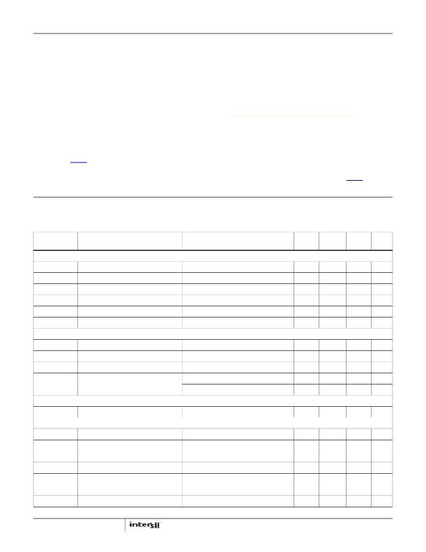
Absolute Maximum Ratings (T A = 25°C)
Thermal Information
Supply Voltage (V S + to V S -) . . . . . . . . . . . . . . . . . . . . . . . . . . .+18V
Thermal Resistance
θ JA (°C/W)
θ JC (°C/W)
Input Voltage . . . . . . . . . . . . . . . . . . . . . . . . . . V S - -0.3V, V S + +0.3V
Continuous Output Current . . . . . . . . . . . . . . . . . . . . . . . . . . 100mA
Storage Temperature Range . . . . . . . . . . . . . . . . . .-65°C to +150°C
16 Ld QFN (Notes 4, 5) . . . . . . . . . . . . 43 5
16 Ld SOIC (Notes 6, 7). . . . . . . . . . . . 73 45
16 Ld QSOP (Note 6). . . . . . . . . . . . . . 112 N/A
Ambient Operating Temperature . . . . . . . . . . . . . . . .-40°C to +85°C
Maximum Die Temperature . . . . . . . . . . . . . . . . . . . . . . . . . . +125°C
Power Dissipation . . . . . . . . . . . . . . . . . . . . . . . . . . . . . See Curves
Pb-Free Reflow Profile. . . . . . . . . . . . . . . . . . . . . . . . .see link below
http://www.intersil.com/pbfree/Pb-FreeReflow.asp
CAUTION: Do not operate at or near the maximum ratings listed for extended periods of time. Exposure to such conditions may adversely impact product reliability and
result in failures not covered by warranty.
NOTES:
4. θ JA is measured in free air with the component mounted on a high effective thermal conductivity test board with “direct attach” features. See
Tech Brief TB379 .
5. For θ JC , the “case temp” location is the center of the exposed metal pad on the package underside.
6. θ JA is measured with the component mounted on a high effective thermal conductivity test board in free air. See Tech Brief TB379 for details.
7. For θ JC , the “case temp” location is taken at the package top center.
IMPORTANT NOTE: All parameters having Min/Max specifications are guaranteed. Typical values are for information purposes only. Unless otherwise noted, all tests
are at the specified temperature and are pulsed tests, therefore: T J = T C = T A
Electrical Specifications
V S + = +5V, V S - = -5V, V H = +5V, V L = -5V, T A = 25°C, unless otherwise specified.
MIN
MAX
PARAMETER
DESCRIPTION
CONDITION
(Note 8)
TYP
(Note 8)
UNIT
INPUT
V IH
Logic “1” Input Voltage
2.0
V
I IH
V IL
I IL
C IN
R IN
Logic “1” Input Current
Logic “0” Input Voltage
Logic “0” Input Current
Input Capacitance
Input Resistance
V IH = 5V
V IL = 0V
0.1
0.1
3.5
50
10
0.8
10
μA
V
μA
pF
M Ω
OUTPUT
R OH
R OL
I LEAK
I PK
ON Resistance V H to OUTx
ON Resistance V L to OUTx
Output Leakage Current
Peak Output Current
I OUT = -100mA
I OUT = +100mA
V H = V S +, V L = V S -
Source
4.5
4
0.1
2.0
6
6
10
Ω
Ω
μA
A
POWER SUPPLY
Sink
2.0
A
I S
Power Supply Current
Inputs = V S +
0.5
1.5
mA
SWITCHING CHARACTERISTICS
t R
t F
t RF Δ
t D +
t D -
t DD
t ENABLE
Rise Time
Fall Time
t R , t F Mismatch
Turn-Off Delay Time
Turn-On Delay Time
t D-1 - t D-2 Mismatch
Enable Delay Time
C L = 1000pF
C L = 1000pF
C L = 1000pF
C L = 1000pF
C L = 1000pF
C L = 1000pF
13.5
13
0.5
12.5
14.5
2
12
ns
ns
ns
ns
ns
ns
ns
3
FN7288.4
January 26, 2012
发布紧急采购,3分钟左右您将得到回复。
相关PDF资料
EL7513IYZ-T7
IC LED DRIVR WHITE BCKLGT 8-MSOP
EL7630ICZ-T7A
IC LED DRVR WHITE BCKLGT SC-70-6
EPG7236
PANEL STEEL 70.2 X 34.2"
ER2-4M-90
EMULATOR EPROM ECONOROM II 4MEG
ER3-8M
EMULATOR EPROM ECONOROM III 8MEG
ESF2424
FRAME SWING ECLIPSE 19.25X19"
ESF3024
FRAME SWING ECLIPSE 24.5X19"
ESF3624
FRAME SWING ECLIPSE 29.75X19"
相关代理商/技术参数
EL7457CSZ
制造商:Intersil Corporation 功能描述:IC MOSFET DRIVER QUAD
EL7457CSZ-T13
功能描述:功率驱动器IC EL7457CSZ 40MHZ ULTR HI SPD CMOS DRVR RoHS:否 制造商:Micrel 产品:MOSFET Gate Drivers 类型:Low Cost High or Low Side MOSFET Driver 上升时间: 下降时间: 电源电压-最大:30 V 电源电压-最小:2.75 V 电源电流: 最大功率耗散: 最大工作温度:+ 85 C 安装风格:SMD/SMT 封装 / 箱体:SOIC-8 封装:Tube
EL7457CSZ-T7
功能描述:功率驱动器IC EL7457CSZ 40MHZ ULTR HI SPD CMOS DRVR RoHS:否 制造商:Micrel 产品:MOSFET Gate Drivers 类型:Low Cost High or Low Side MOSFET Driver 上升时间: 下降时间: 电源电压-最大:30 V 电源电压-最小:2.75 V 电源电流: 最大功率耗散: 最大工作温度:+ 85 C 安装风格:SMD/SMT 封装 / 箱体:SOIC-8 封装:Tube
EL7457CSZ-T7A
功能描述:功率驱动器IC EL7457CSZ 40MHZ ULTR HI SPD CMOS DRV 250P RoHS:否 制造商:Micrel 产品:MOSFET Gate Drivers 类型:Low Cost High or Low Side MOSFET Driver 上升时间: 下降时间: 电源电压-最大:30 V 电源电压-最小:2.75 V 电源电流: 最大功率耗散: 最大工作温度:+ 85 C 安装风格:SMD/SMT 封装 / 箱体:SOIC-8 封装:Tube
EL7457CU
功能描述:IC DVR CMOS QUAD 40MHZ 16-QSOP RoHS:否 类别:集成电路 (IC) >> PMIC - MOSFET,电桥驱动器 - 外部开关 系列:- 标准包装:50 系列:- 配置:低端 输入类型:非反相 延迟时间:40ns 电流 - 峰:9A 配置数:1 输出数:1 高端电压 - 最大(自引导启动):- 电源电压:4.5 V ~ 35 V 工作温度:-40°C ~ 125°C 安装类型:表面贴装 封装/外壳:TO-263-6,D²Pak(5 引线+接片),TO-263BA 供应商设备封装:TO-263 包装:管件
EL7457CU-T13
功能描述:IC DRIVER QUAD 40MHZ HS 16-QSOP RoHS:否 类别:集成电路 (IC) >> PMIC - MOSFET,电桥驱动器 - 外部开关 系列:- 标准包装:50 系列:- 配置:低端 输入类型:非反相 延迟时间:40ns 电流 - 峰:9A 配置数:1 输出数:1 高端电压 - 最大(自引导启动):- 电源电压:4.5 V ~ 35 V 工作温度:-40°C ~ 125°C 安装类型:表面贴装 封装/外壳:TO-263-6,D²Pak(5 引线+接片),TO-263BA 供应商设备封装:TO-263 包装:管件
EL7457CU-T7
功能描述:IC DRIVER QUAD 40MHZ HS 16-QSOP RoHS:否 类别:集成电路 (IC) >> PMIC - MOSFET,电桥驱动器 - 外部开关 系列:- 标准包装:50 系列:- 配置:低端 输入类型:非反相 延迟时间:40ns 电流 - 峰:9A 配置数:1 输出数:1 高端电压 - 最大(自引导启动):- 电源电压:4.5 V ~ 35 V 工作温度:-40°C ~ 125°C 安装类型:表面贴装 封装/外壳:TO-263-6,D²Pak(5 引线+接片),TO-263BA 供应商设备封装:TO-263 包装:管件
EL7457CUZ
功能描述:功率驱动器IC EL7457CUZ 40MHZ ULTR HI SPD CMOS DRVR RoHS:否 制造商:Micrel 产品:MOSFET Gate Drivers 类型:Low Cost High or Low Side MOSFET Driver 上升时间: 下降时间: 电源电压-最大:30 V 电源电压-最小:2.75 V 电源电流: 最大功率耗散: 最大工作温度:+ 85 C 安装风格:SMD/SMT 封装 / 箱体:SOIC-8 封装:Tube
